
Product
FRIENDLY/link Nantong zhuolida Ali SAMSAN Corrosion machining Nantong zhuolida HJD Shenzhen zhuolida Esprit print
HOTLINE
189-3869-3452 0513-8160 1666

189-3869-3452 0513-8160 1666

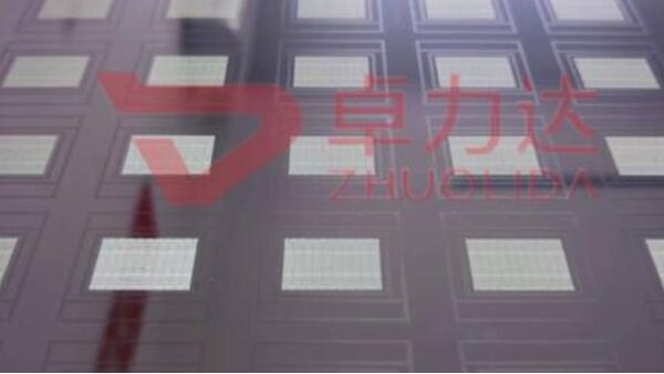
With the rapid iteration of semiconductor packaging technology, high-end fields such as 5G communication, automotive electronics, artificial intelligence, and energy storage chips have continuously raised stringent requirements for the precision, stability, and yield ofIC substrate packaging processes. As a core supporting component for solder paste printing, ball mounting coating, and high-precision packaging, the IC substrate packaging stencil directly determines the quality of chip packaging through its opening accuracy, hole wall verticality, and plate flatness, serving as a key accessory to avoid soldering defects including bridging, virtual soldering, and missing printing. Traditional packaging stencils manufactured by laser cutting and etching processes can no longer meet the high-end packaging demands for high density, ultra-fine apertures, and ultra-thin plates. Located in the core precision manufacturing hub of the Yangtze River Delta, Nantong Zhuolida has long specialized in precision electroforming technology. Focusing on customized high-precisionIC substrate packaging stencils, electroforming packaging stencils, and semiconductor packaging stencils, the company solves industrial high-precision packaging processing pain points with differentiated technological advantages and provides localized high-quality domestic packaging supporting solutions for semiconductor enterprises in Nantong and the broader Yangtze River Delta region.
Most conventional semiconductor packaging stencils on the market are produced by etching and laser cutting processes, which show obvious limitations in high-end IC substrate packaging scenarios. Restricted by the subtractive chemical processing principle, the etching process inevitably causes undercutting, forming trumpet-shaped openings with inclined and rough hole walls. In ultra-fine pitch and high-density array opening operations, it easily leads to poor solder paste demolding and solder residue, resulting in mass bridging and virtual soldering defects and greatly reducing the packaging yield rate. Laser cutting is a thermal processing technology. High-temperature burning generates oxidation slag and tiny burrs on the edges of openings. Subsequent polishing tends to damage micro-pore structures, while the processing process may cause deformation of ultra-thin stencils and offset hole positions, failing to meet the micron-level precision standards for precision substrate packaging.
In addition, traditional processes suffer from poor mass production consistency, with deviations in aperture size and plate flatness between batches, making them incompatible with standardized automated pipeline production. For a long time, high-end domesticIC substrate packaginghave relied on imports, which are accompanied by high procurement costs, long delivery cycles, and delayed after-sales commissioning responses. These problems severely restrict the efficient development of the local semiconductor packaging industry, creating an urgent demand for cost-effective and highly stable domestic precision electroforming packaging stencils as an alternative.
Precision electroforming technology is currently the optimal solution for manufacturing high-endIC substrate packagingstencils. Adopting the additive molding principle of electrochemical ion deposition, it completely overcomes the shortcomings of traditional subtractive processing and perfectly adapts to high-precision semiconductor packaging requirements. Compared with traditional technologies, electroforming packaging stencils are molded at low temperatures without mechanical extrusion or high-temperature thermal damage, resulting in zero internal stress and flat, warp-free ultra-thin plates that fit automated printing equipment accurately and ensure stable packaging operations. The stencil openings are precisely replicated through ultra-precision master molds, featuring vertical and smooth hole walls without burrs or undercut deviations, fundamentally eliminating industrial problems such as solder paste clogging, uneven demolding, and printing offset.
In terms of precision control, the aperture tolerance of electroformed semiconductor packaging stencils is stably controlled within ±1μm, with uniform hole spacing and excellent array consistency. It supports customized complex structures including ultra-fine micro-pores, high-density array holes, and special-shaped openings, adapting to various high-end chip substrate packaging scenarios such as BGA, CSP, FC, and WLCSP. Meanwhile, electroformed stencils feature dense and uniform metal structure, high surface smoothness, excellent wear and corrosion resistance, and no deformation or wear after repeated printing. Their service life is far longer than products made by traditional processes, effectively reducing consumable replacement costs for enterprises.
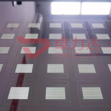
Semiconductor packaging is a high-precision and high-cleanliness production scenario with strict requirements for the cleanliness and stability of supporting stencils. As a local original manufacturer in Nantong, Nantong Zhuolida has built an exclusive dust-free electroforming production workshop and established a semiconductor-grade full-process quality control system. Covering master mold production, high-purity solution proportioning, intelligent electrodeposition, low-temperature demolding, dust-free cleaning, precision passivation, and precision testing, all processes are independently controlled without outsourcing, effectively avoiding quality defects such as impurities, pinholes, and loose coatings from the source.
The production line is equipped with an intelligent current regulation system and multi-stage circulating filtration and degassing equipment to balance the metal deposition rate and ensure uniform thickness and dense structure of each packaging stencil. Finished products undergo ultrasonic ultra-pure water dust-free cleaning and full-size inspection via high-precision vision detectors to strictly verify aperture accuracy, hole spacing deviation, and plate flatness. This ensures zero deviation, high cleanliness, and high stability of batch products, fully complying with the mass production working conditions of semiconductor dust-free workshops.
Adjacent to core semiconductor industrial clusters including Shanghai, Suzhou, and Wuxi, Nantong boasts unique supply chain location advantages and can efficiently serve semiconductor packaging enterprises in surrounding cities. Compared with imported products, local manufacturers support rapid sampling, process commissioning, and batch delivery, greatly shortening delivery cycles and reducing procurement costs. One-on-one professional process optimization services are provided to customize exclusive electroforming packaging stencil solutions according to actual substrate packaging working conditions, with professional DFM structural optimization suggestions to effectively avoid production risks.
Benefiting from years of dual-process technical accumulation in electroforming and etching, the enterprise flexibly matches optimal processes for both conventional and high-precision packaging needs, efficiently supporting both new product R&D sampling and large-scale stable mass production. With the core advantages of high precision, high yield, and cost performance, its products are gradually replacing imported alternatives, helping the Yangtze River Delta semiconductor packaging industry improve quality and efficiency and promoting the localization upgrading of high-precision packaging components.
Conclusion
As semiconductor packaging technology continues to upgrade toward miniaturization, high density, and high cleanliness, precision electroforming IC substrate packagingstencils have become standard core equipment for high-end packaging production lines. Featuring vertical micro-pores, zero burrs, stress-free deformation, and superior batch consistency, they completely solve the packaging pain points of traditional stencils and significantly improve chip packaging yield rates. Rooted in Nantong and serving the entire Yangtze River Delta, local precision electroforming manufacturers continue to provide high-quality customized semiconductor packaging stencil solutions for semiconductor enterprises with mature technology, dust-free mass production capacity, and efficient localized services, empowering the high-quality development of the domestic high-precision packaging industry.

 189-3869-3452 0513-8160 1666
 E-MAIL:yw5@zldsmt.com
 QQ:$qq
 No. 268, Jinchuan Road, Nantong high tech Industrial Development Zone, Tongzhou District, Nantong City, Jiangsu Province
All Rights Reserved © 2019-2030Nantong Zhuolida metal Technology Co., Ltd.
ICP:【苏ICP备17060045号-3】


 TEL
TEL Products
 News
News About us