
Product
FRIENDLY/link Nantong zhuolida Ali SAMSAN Corrosion machining Nantong zhuolida HJD Shenzhen zhuolida Esprit print
HOTLINE
189-3869-3452 0513-8160 1666

189-3869-3452 0513-8160 1666

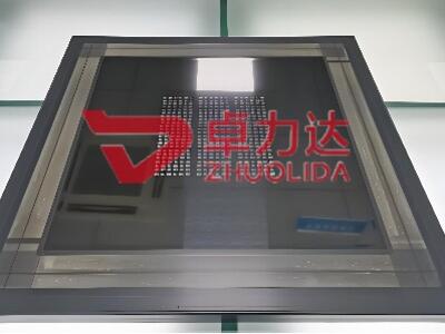
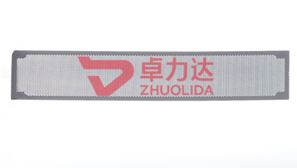
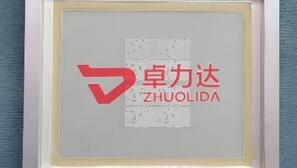
With the rapid upgrading of advanced semiconductor packaging, driven by AI computing, 5G communication, and high-speed HBM memory technology, ABF substrates have become the core carrier for high-density, high-precision IC packaging. As critical auxiliary tooling for FC-BGA, AI chip, and HBM packaging production, ABF substrate ball placement stencils directly determine packaging yield, dimensional consistency, and long-term operational reliability. Traditional etching stencils can no longer adapt to ultra-fine pitch and micro-aperture processing demands, making precision electroforming technology the mainstream solution for high-end semiconductor packaging stencil manufacturing. Nantong Zhuolida focuses on electroforming precision processing, delivering high-performance ABF ball placement stencils to empower global advanced packaging industries with higher accuracy and stability.
Different from ordinary stainless steel stencils, electroformed ABF substrate ball placement stencils adopt additive electrochemical deposition molding, featuring ultra-high hole position accuracy, ultra-smooth hole wall finish, and stable structural tension. The precision-controlled aperture tolerance effectively eliminates common packaging defects such as solder ball clogging, solder bridging, and offset deviation. With excellent demolding performance, the stencils ensure uniform solder paste release and consistent ball placement effect in mass production, perfectly matching the ultra-fine pitch packaging standards of modern AI chips, high-end FC-BGA devices, and HBM high-density memory substrates.
Nantong Zhuolida’s professional electroforming process significantly improves stencil durability and structural stability. The nickel-cobalt alloy electroformed layer features high hardness, strong wear resistance, and non-deformation performance during long-term continuous printing. Compared with conventional etched stencils, our customized ABF substrate ball placement stencils greatly reduce replacement frequency, lower production downtime, and cut comprehensive manufacturing costs for semiconductor manufacturers. All products undergo full-precision dimensional inspection before delivery, achieving outstanding batch consistency to meet strict large-scale mass production requirements of advanced packaging lines.
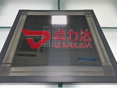
We support full-custom drawing services for diverse ABF substrate specifications, providing rapid prototyping and stable batch delivery. Relying on 18 years of precision electroforming experience and military-grade quality control systems, Nantong Zhuolida optimizes stencil aperture structure, thickness distribution, and tension balance for different packaging scenarios. Whether for consumer electronics AI chips, automotive electronic packaging, or high-end server HBM storage packaging, our ABF substrate ball placement stencils maintain excellent printing stability and ball placement accuracy.
In the fiercely competitive advanced semiconductor packaging field, precision tooling is the core foundation of technological iteration and yield improvement. Adhering to innovation-driven and quality-oriented development, Nantong Zhuolida continuously optimizes precision electroforming craftsmanship, breaks through the precision bottlenecks of traditional stencil manufacturing, and provides reliable, high-precision, and cost-effective ABF substrate ball placement stencils solutions for global semiconductor customers. Committed to becoming a trusted long-term partner in advanced packaging tooling, we keep elevating industry standards for semiconductor precision packaging.

 189-3869-3452 0513-8160 1666
 E-MAIL:yw5@zldsmt.com
 QQ:$qq
 No. 268, Jinchuan Road, Nantong high tech Industrial Development Zone, Tongzhou District, Nantong City, Jiangsu Province
All Rights Reserved © 2019-2030Nantong Zhuolida metal Technology Co., Ltd.
ICP:【苏ICP备17060045号-3】


 TEL
TEL Products
 News
News About us