HOTLINE

189-3869-3452 0513-8160 1666
  • Stencils for IC Substrate Packaging
1/1
Stencils for IC Substrate Packaging
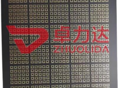
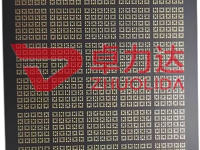
Nantong Zhuolida produces IC substrate packaging stencils for BGA, CSP, FC and SiP. Adopting laser cutting and electroforming, our stainless steel & nickel-cobalt stencils ensure precise printing with fewer defects. Custom stepped and nano-coated stencils available. We support quick sampling and bulk supply for memory, power and RF semiconductor packaging.

189-3869-3452 0513-8160 1666

PRODUCT DETAILS

High-Precision IC Substrate Packaging Stencils for Semiconductor Advanced Packaging

As advanced semiconductor packaging evolves toward miniaturization, high density and ultra-fine pitch, IC substrate bumping stencils have become indispensable tooling for reliable solder paste printing and flux transfer. Poor stencil precision easily triggers bridging, missing prints and inconsistent solder volume, directly lowering packaging yield. Nantong Zhuolida specializes in custom manufacturing  IC substrate bumping stencils, IC substrate bumping stencils and electroformed stencils tailored to modern chip packaging demands.

Our stencil solutions support mainstream packaging architectures including BGA, CSP, Flip Chip (FC) and SiP, fully meeting the stringent requirements of solder paste printing and conductive paste transfer on high-density, fine-pitch IC substrates. In high-end packaging production, minor deviations in aperture shape, dimensional stability and sidewall smoothness will be amplified during mass printing. For this reason, we adopt two mature core manufacturing technologies: precision laser cutting and professional electroforming.

Electroformed stencils stand out for ultra-smooth trapezoidal aperture walls, superior dimensional accuracy and consistent opening tolerance. Compared with conventional laser-cut stencils, electroformed nickel stencils deliver cleaner solder release, less paste adhesion and stable printing performance for ultra-fine apertures. Laser-cut stainless steel stencils offer cost advantages for medium pitch applications, suitable for diversified mass-production packaging lines. Both processes ensure uniform solder deposition and smooth demolding during continuous printing, effectively reducing common defects such as solder bridging, missing pads and insufficient paste volume, greatly improving overall packaging yield.

168899a6f0ed4fcf81055724aa17cc57_34
Material selection is critical for long-term stable printing performance. Nantong Zhuolida provides premium stainless steel and nickel-cobalt alloy stencils. Nickel-cobalt electroformed stencils feature higher hardness, outstanding wear resistance and low internal stress, maintaining flatness under long-cycle printing without deformation. All raw materials are strictly inspected to guarantee thermal stability and flatness, avoiding printing distortion caused by thermal expansion during reflow processes.

To satisfy diverse packaging process designs, we supply customized stencil options, including stepped stencils and nano-coated stencils. Stepped stencils solve printing challenges for mixed-size pads on a single IC substrate. Nano coating reduces surface energy of aperture walls, further optimizing paste release and lowering cleaning frequency for production lines. Customers can submit Gerber files, drawings or samples for personalized development according to actual printing parameters, substrate thickness and pitch specifications.

Semiconductor-grade production and inspection standards are implemented throughout our factory. We deploy high-precision optical measuring instruments to inspect aperture dimension, position accuracy and flatness for every finished stencil. Our technical team has rich experience serving memory chips, power semiconductor devices, RF chips and other advanced packaging segments. We support rapid prototyping for new product verification, alongside stable mass delivery for long-term orders.

Many semiconductor packaging manufacturers face persistent pain points: unstable printing consistency from ordinary stencils, frequent bridging on fine-pitch substrates, short service life and long lead time for custom samples. Nantong Zhuolida’s integrated manufacturing capacity resolves these difficulties. We combine electroforming and laser processing under one roof, enabling flexible switching between small-batch R&D samples and large-volume repetitive orders.

Whether you require standard IC substrate bumping stencils, ultra-precision electroformed bumping stencils or special functional coated stencils, we provide one-stop technical consultation, design optimization, production and after-sales support. If you are looking for a reliable China-based manufacturer of IC substrate bumping stencils with strict quality control and competitive lead time, contact Nantong Zhuolida for detailed quotations and free technical discussion.


PRODUCT CHARACTERISTICS

HOT PRODUCT
Microporous filter

Microporous filter

A microporous filter is a device that uses a microporous filter membrane to filter, which is mainly used to separate particles and microorganisms in liquids or gases.
Seamless welding

Seamless welding

Seamless welding plays a key role in different industries, helping parts and other products to improve the accuracy, finish, beauty of products, and effectively shorten the production and processing cycle of the overall mold.
Chemical etching

Chemical etching

Chemical etching processing can be used to produce copper plate, zinc plate and other printed plate concave and convex, also widely used to reduce the weight of instrument panels, and traditional processing methods difficult to process thin workpiece processing.After continuous improvement and the development of process equipment, it can also be used in the aviation, machinery, chemical industry electronic chip parts precision etching products processing, especially in the semiconductor process, etching is an indispensable technology.
Corrosion of molybdenum

Corrosion of molybdenum

Molybdenum corrosion processing is used in various fields of national economy, such as aerospace and nuclear energy, lighting and electronic devices, vacuum furnace and protective atmosphere furnace, metal pressure processing glass industry, etc